-
Products
- Application
- Company
-
Services
- Resources
- News
-
Contact Us

1. PNP Configuration: The transistor operates in a PNP configuration, making it suitable for use in complementary circuits.
2. High Current Gain: The device has a high current gain (hFE) of up to 700, which makes it suitable for use in low-power amplification circuits.
3. Low Noise: The SS8550DBU transistor has a low noise level, making it ideal for use in low noise amplifier circuits.
4. Small Signal Amplification: The device can be used in small signal amplification such as audio amplifiers, voltage regulators, and switching applications.
5. High Breakdown Voltage: The transistor has a high breakdown voltage of up to -25V, which makes it ideal for use in high voltage circuits.
6. Bipolar Junction Transistor: The device is a bipolar junction transistor (BJT), which means it is a current-controlled device and can switch on and off quickly.
7. Small Size: The device has a small size and can be mounted on a small PCB or a breadboard.
8. RoHS Compliant: The transistor is RoHS compliant, which means it does not contain any hazardous substances.
9. Wide Temperature Range: The SS8550DBU transistor has a wide operating temperature range of -55°C to +150°C, making it suitable for use in extreme environments.
10. Low Cost: The SS8550DBU transistor is low-cost and widely available, making it ideal for use in low-cost electronic devices.
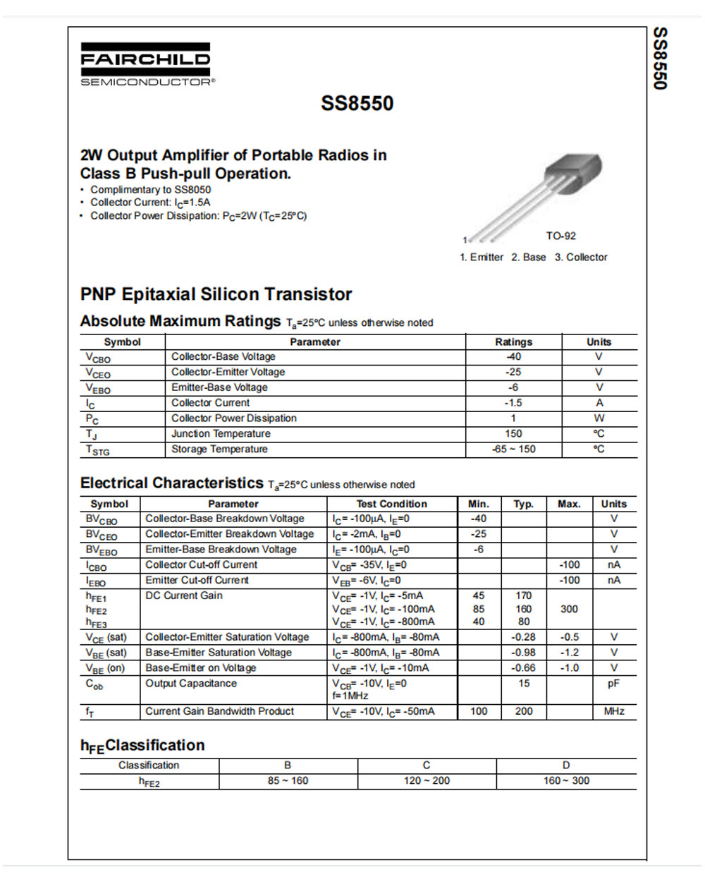
Complimentary to SS8050
Collector Current: IC=1.5A
Collector Power Dissipation: PC=2W (TC=25℃)
Ta=25℃ unless otherwise noted
Symbol | Parameter | Ratings | Units |
VCBO | Collector-Base Voltage | -40 | V |
VCEO | Collector-Emitter Voltage | -25 | V |
VEBO | Emitter-Base Voltage | -6 | V |
IC | Collector Current | -1.5 | A |
PC | Collector Power Dissipation | 1 | W |
TJ | Junction Temperature | 150 | ℃ |
TSTG | Storage Temperature | -65~150 | ℃ |
Ta=25°Cunless otherwise noted
Symbol | Parameter | Test Condition | Min. | Typ. | Max. | Units |
BVCBO | Collector-Base Breakdown Voltage | IC=-100μA, IE=0 | -40 | V | ||
BVCEO | Collector-Emitter Breakdown Voltage | IC=-2mA, IB=0 | -25 | V | ||
BVEBO | Emitter-Base Breakdown Voltage | IE=-100μA, IC=0 | -6 | V | ||
ICBO | Collector Cut-off Current | VCB=-35V, IE=0 | -100 | nA | ||
IEBO | Emitter Cut-off Current | VEB=-6V, IC=0 | -100 | nA | ||
hFE1 hFE2 hFE3 | DC Current Gain | VCE=-1V, IC=-5mA VCE=-1V, IC=-100mA VCE=-1V, IC=-800mA | 45 85 40 | 170 160 80 | 300 | |
VCE(sat) | Collector-Emitter Saturation Voltage | IC=-800mA, IB=-80mA | -0.28 | -0.5 | V | |
VBE(sat) | Base-Emitter Saturation Voltage | IC=-800mA, IB=-80mA | -0.98 | -1.2 | V | |
VBE(on) | Base-Emitter on Voltage | VCE=-1V, IC=-10mA | -0.66 | -1.0 | V | |
Cob | Output Capacitance | VCB=-10V, IE=0 f=1MHz | 15 | pF | ||
fT | Current Gain Bandwidth Product | VCE=-10V, IC=-50mA | 100 | 200 | MHz |
Classification | B | C | D |
hFE2 | 85~160 | 120~200 | 160~300 |


