-
Products
- Application
- Company
-
Services
- Resources
- News
-
Contact Us

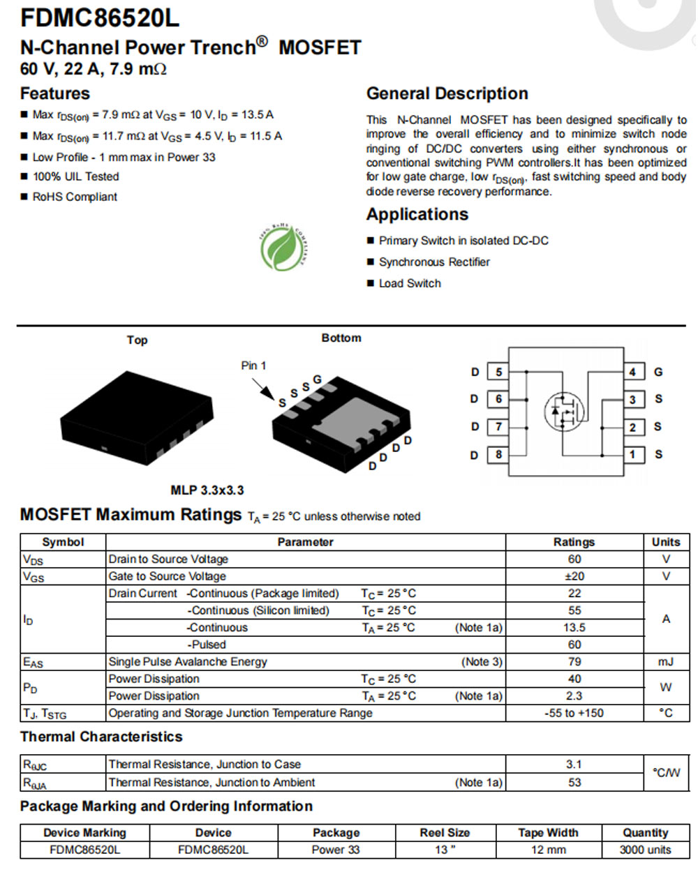
Max rDS(on) = 7.9 mΩ at VGS = 10 V, ID = 13.5 A
Max rDS(on) = 11.7 mΩ at VGS = 4.5 V, ID = 11.5 A
Low Profile - 1 mm max in Power 33
100% UIL Tested
RoHS Compliant
This N-Channel MOSFET has been designed specifically to improve the overall efficiency and to minimize switch node ringing of DC/DC converters using either synchronous or conventional switching PWM controllers. lt has been optimized for low gate charge, low rDS(on, fast switching speed and body diode reverse recovery performance.
Primary Switch in isolated DC-DC
Synchronous Rectifier
Load Switch
TA=25℃ unless otherwise noted
Symbol | Parameter | Ratings | Units |
VDS | Drain to Source Voltage | 60 | V |
VGS | Gate to Source Voltage | ±20 | V |
lD | Drain Current - Continuous(Package limited) TC=25℃ | 22 | A |
- Continuous (Silicon limited) TC=25℃ | 55 | ||
- Continuous TA=25℃ (Note 1a) | 13.5 | ||
- Pulsed | 60 | ||
EAs | Single Pulse Avalanche Energy (Note 3) | 79 | mJ |
Po | Power Dissipation TC=25℃ | 40 | W |
Power Dissipation TA=25℃ (Note 1a) | 2.3 | ||
TJ, TSTG | Operating and Storage Junction Temperature Range | -55 to +150 | ℃ |
RθJC | Thermal Resistance, Junction to Case | 3.1 | ℃/W |
RθJA | Thermal Resistance, Junction to Ambient (Note 1a) | 53 |
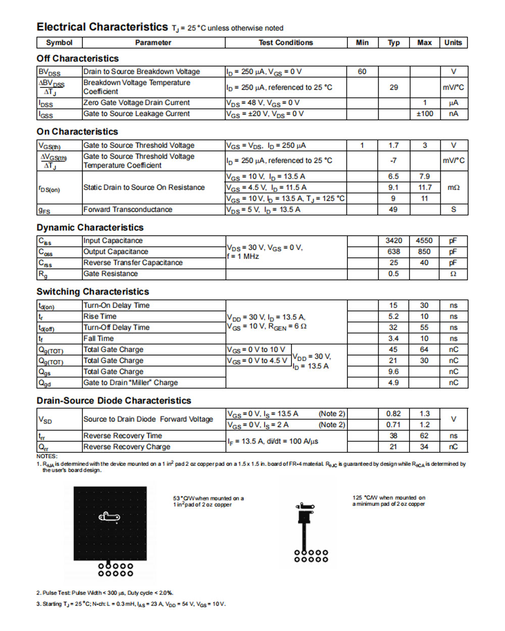
TJ=25℃ unless otherwise noted
Symbol | Parameter | Test Conditons | Min | Typ | Max | Units |
BVDSS | Drain to Source Breakdown Voltage | ID=250μA, VGS=0V | 60 | V | ||
△BVDSS —— △TJ | Breakdown Voltage Temperature Coefficient | ID=250μA, referenced to 25℃ | 29 | mV/℃ | ||
IDSS | Zero Gate Voltage Drain Curent | VDS=48 V, VGS=0V | 1 | μA | ||
IGSS | Gate to Souroe Leakage Current | VGS=±20V, VDS=0V | ±100 | nA |
VGS(th) | Gate to Souroe Threshold Voltage | VGS=VDS, ID=250 μA | 1 | 1.7 | 3 | V |
△VGS(th) —— △TJ | Gate to Source Threshold Voltage Temperature Coeficient | ID=250μA, referenced to 25℃ | -7 | mV/℃ | ||
rDS(on) | Static Drain to Source On Resistanoe | VGS=10V, ID=13.5 A | 6.5 | 7.9 | mΩ | |
VGS=4.5V. ID=11.5A | 9.1 | 11.7 | ||||
VGS=10V, ID=13.5A. TJ=125℃ | 9 | 11 | ||||
gFS | Forward Transconductance | VDS=5V, ID=13.5A | 49 | S |
Clss | Input Capacitance | VDS=30V, VGS=0V, f=1 MHz | 3420 | 4550 | pF | |
Coss | Output Capacitance | 638 | 850 | pF | ||
Crss | Reverse Transfer Capacitance | 25 | 40 | pF | ||
Rg | Gate Resistance | 0.5 | Ω |
td(on) | Turn-On Delay Time | VDD=30V ID=13.5A VGS=10V, RGEN=6Ω | 15 | 30 | ns | ||
tr | Rise Time | 5.2 | 10 | ns | |||
td(off) | Turn-Of Delay Time | 32 | 55 | ns | |||
tr | Fall Time | 3.4 | 10 | ns | |||
Qg(TOT) | Total Gate Charge | VGS=0V to 10V | VDD=30V | 45 | 64 | nC | |
Qg(TOT) | Total Gate Charge | VGS=0V to 4.5V | 21 | 30 | nC | ||
Qgs | Total Gate Charge | ID=13.5A | 9.6 | nC | |||
Qgd | Gate to Drain "Miller" Charge | 4.9 | nC | ||||
VSD | Source to Drain Diode Forward Voltage | VGS=0V, IS=13.5A (Note 2) | 0.82 | 1.3 | V | |
VGS=0V, IS=2 A (Note 2) | 0.71 | 1.2 | ||||
trr | Reverse RecoveryTime | lF=13.5A, di/dt=100 A/μs | 38 | 62 | ns | |
Qrr | Reverse Recovery Charge | 21 | 34 | nC |
NOTES:
1. RθJA is determined with the device mounted on a 1 in2 pad 2 oz copper pad on a 1.5 x 1.5 in. board of FR-4 material RθJC is guaranteed by design while RθCA is determined by the user's board design.
2. PulseTest: Pulse Width<300μs, Duty cycle<2.0%.
3. Starting TJ=25℃; N-ch: L=0.3mH, IAS=23A, VDD=54V, VQS=10V.


