-
Products
- Application
- Company
-
Services
- Resources
- News
-
Contact Us

The plastic package carries Underwriters Laboratory Flammability Classification 94V-0 Idea
For printed circuit board
Super fast switching for high efficiency
Low reverse leakage
High forward surge current capability
High temperature soldering guaranteed 250℃/ 10 seconds at terminals
Case: JEDEC DO-41 Molded plastic body
Terminals: Solder plated, solderable per MlL-STD-750, Method 2026
Polarity: Polarity symbol marking on body
Mounting Position: Any
Weight: 0.012 ounce, 0.33 grams
Ratings at 25°C ambient temperature unless otherwise specified.
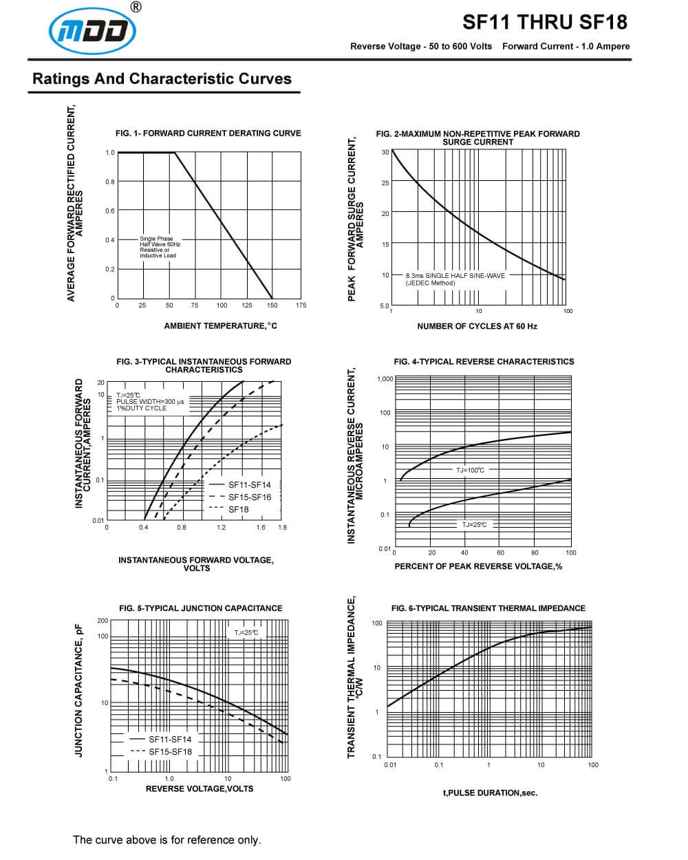
Single phase half-wave 60Hz, resistive or inductive load, for capacitive load current derate by 20%
Parameter | SYMBOLS | SF11 | SF12 | SF13 | SF14 | SF15 | SF16 | SF18 | UNITS |
Marking Code | MDD SF11 | MDD SF12 | MDD SF13 | MDD SF14 | MDD SF15 | MDD SF16 | MDD SF18 | ||
Maximum repetitive peak reverse voltage | VRRM | 50 | 100 | 150 | 200 | 300 | 400 | 600 | V |
Maximum RMS voltage | VRMS | 35 | 70 | 105 | 140 | 210 | 280 | 420 | V |
Maximum DC blocking voltage | VDC | 50 | 100 | 150 | 200 | 300 | 400 | 600 | V |
Maximum average forward rectified current at TA=55℃ | I(AV) | 1.0 | A | ||||||
Peak forwardsurge current 8.3ms single half sine-wave superimposed onrated load (JEDEC Method) | IFSM | 30.0 | A | ||||||
Maximum instantaneous forward voltage at 1.0A | VF | 0.95 | 1.25 | 1.7 | V | ||||
Maximum DC reverse current TA=25℃ at rated DC blocking voltage TA=100℃ | IR | 5.0 50.0 | μA | ||||||
Maximum reverse recovery time (NOTE 1) | trr | 35 | ns | ||||||
Typical junction capacitance (NOTE 2) | CJ | 15.0 | 10.0 | pF | |||||
Typical thermal resistance (NOTE 3) | RθJA | 60.0 | ℃/W | ||||||
Operating junction and storage temperature range | TJ,TSTG | -65 to+150 | ℃ | ||||||
Note:1.Reverse recovery condition IF=0.5A,IR=1.0A,Irr=0.25A
2. Measured at 1MHz and applied reverse voltage of 4.0V D.C.
3. Thermal resistance from junction to ambient at 0.375"(9.5mm) lead length, P.C.B. mounted


